Faculty Research: Printing in Reverse
Professor Nick Fang Explores Etching at the Nanoscale
 |
 |
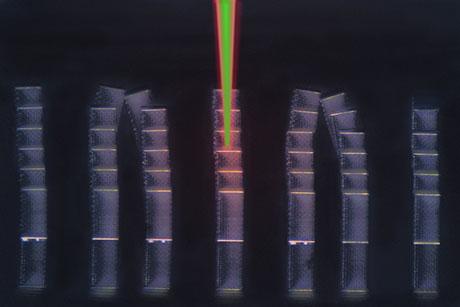
| Using electrochemical and optical processes, programmable metamaterials, composed of functional micro- and nanostructures, are prototyped at Fang’s lab for applications such as reducing thermal expansion, trapping, and steering waves. Credit: Tony Pulsone | Fang’s group studies manufacturable components and devices for concentrating light at the nanoscale. Their applications span from imaging to energy conversion. Credit: Tony Pulsone |
by Alissa Mallinson
Have you ever wondered how your favorite DVD was created? Nanostructure printing on plastics and polymers is nothing new. But what about on metal or glass—for electronic circuit boards, for example? “Electrochemical machining works on the micro scale,” says Nicholas X. Fang, the d’Arbeloff Career Development Associate Professor, “but not yet on the nano scale. The requirement is 100 times off, because if you try to apply a voltage across liquid and metal, it spreads out and smears small features.”
Fang and his group searched for harder materials to print on for use in electronics, photonics, and fiber optics (his expertise is in nanophotonics and nanomanufacturing), but in the process they discovered something entirely new. Instead of creating an impression on polymer, as happens with pressing, the group developed a process of etching that allows for nanoscale-level precision on hard materials. It is also a speedy, low-voltage process.
Etching occurs when a solid stamp is covered with an electrode that connects to the positive pole of a battery, while the material to be etched is connected to the negative pole. When the circuit is switched on, the electrons are repelled from the material, leaving active ions on the surface. These ions are then pulled toward the positive electrode in the stamp, leaving an empty space where they used to be in the pattern of the stamp.
The materials for both the stamp and the material are of the utmost importance, requiring specific electrochemical and mechanical properties to allow the etching to occur. The group’s favorite is Nafion (an ion-conducting polymer commonly used in batteries and fuel cells), because it can incorporate several types of ions and chemical species. Fang says, “We have to select the stamp materials based on particular electrochemical and mechanical properties, since we want to shape the stamps with fine nanostructures and maintain their geometry against wear and tear from extended use. That limits the type of materials suited for the stamps, but we are fortunate to have found several that meet our needs. We are still learning tricks from chemistry to expand the list.”
According to Fang, they can print down to 20 nanometers, about 1,000 times smaller than the width of a hair, on curved surfaces (including fibers) as well as flat surfaces, at a rate of up to tens of nanometers per second. That means films of several microns thick can be etched in a few minutes. “It turns out that this process does not rely on hardness of the materials being etched, unlike the counterpart, chemical-mechanical polishing, which does not work well for copper in particular,” he says. “So we have reduced a process that can take up to 8 hours to a couple minutes.”
A major result of Fang’s discovery is the ability to print metal circuit boards at the nanoscale, which previously could only be accomplished on the microscale. Another application is in the area of photonics. “One thing we could now do is selectively enhance the reflection of an infrared wavelength, which we can use to create a smart window that rejects heat in summertime and absorbs more heat from the sun in winter time.”
So far Fang and his team have demonstrated the ability to print on an area of 2 inches, but they anticipate being able to increase that to the size of a window. “We are also trying to build a tool that is compatible with the contact aligners that are used in many semiconductor fabrication designs. In particular, we want to make something as portable and modular as a laptop so you can essentially print the same module and turn it into a nanofabrication system.”
Fang’s new process has important applications as a catalyst for other nano materials as well; for example, etching into silicon to create silicon nano wires or nano patterns. In other words, printing a catalyst that can generate other nano materials.
“We are interested in silicon because silicon nanowires, when properly shaped, can absorb 98% of light over the complete visible range. We are working with a company now to help create a space telescope whose material composition will not fail in space. Since we can now print nanoscale structures on flexible materials like silicon, we are able to help them.”
Other applications include sensors to enhance florescence, thermal imaging, and possible early detection of some dangerous species.![]()


