Nanoscribe GT2 adds to MIT.nano fabrication capabilities
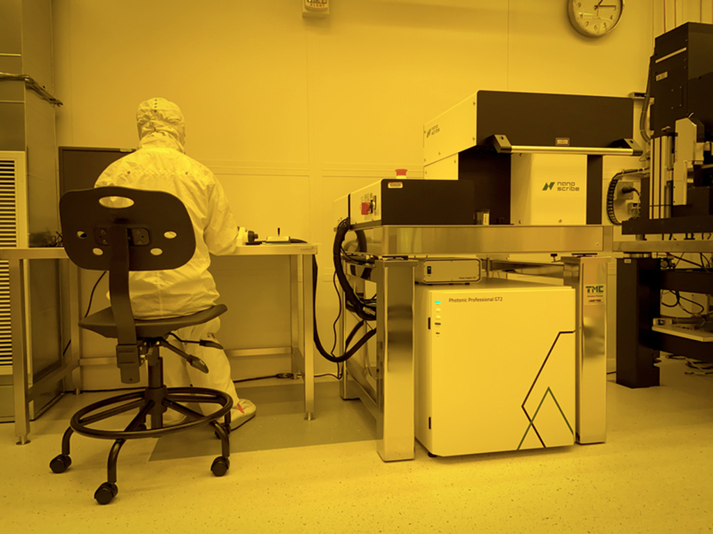
MIT.nano has added the Nanoscribe Photonic Professional GT2, a high-speed, three-dimensional microfabrication instrument, to its fabrication capabilities. The GT2 will provide MIT.nano users with the ability to create high-resolution 3D structures. It has been installed and qualified in MIT.nano’s third-floor soft lithography space, and is now available for training and use.
The GT2 uses two-photon technology to crosslink special polymers and produce intricate structures of nearly any 3D shape, including crystal lattices, porous scaffolds, and naturally inspired patterns. The tool offers this design flexibility while also being incredibly precise — it has a finest resolution down to 400 nanometers. It is also fast; the GT2 has a maximum scan speed of 625 millimeters per second. This tool will support research and rapid prototyping in a variety of areas such as microfluidics, micromechanics, biomedical engineering, micro-optics, and nanostructures.
“The GT2 employs a fundamentally different approach compared to other types of lithography systems we have in the fab,” says Assistant Director for User Services Jorg Scholvin. “It opens up completely new types of devices and research paths that would be impossible to explore with conventional lithography methods.”
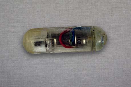
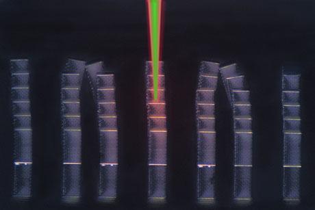
The new instrument was purchased by the Portela Research Group in the Department of Mechanical Engineering. The group, which focuses on architected mechanics and materials across scales, is led by d’Arbeloff Career Development Assistant Professor Carlos Portela. In a recent study led by Portela, researchers fabricated an ultralight “nanoarchitected” material that can withstand supersonic microparticle impacts. “This work marks the beginning of our explorations on the dynamics of nanomaterials, which we plan to do at MIT.nano,” said Portela.
To accompany the new GT2, MIT.nano also acquired a multi-application critical point dryer (CPD) with a 2.5-inch chamber for use with lithography processes. Critical point drying is a process to remove liquid and dry delicate samples in a controlled way. This is particularly important to enable the delicate, sub-micron structures fabricated with the GT2. Forces from surface tension can pull at small, fragile structures as liquids change phase to gas and evaporate, resulting in damaged or destroyed devices. By pushing the pressure-temperature profile of the fluid near the critical point — at which the differences between the gas and liquid phases no longer exist — the sample can be “dried” without crossing these phase boundaries, avoiding damage from surface tension forces.
The new dryer, a Tousimis Autosamdri-931, can process up to five substrates per run and offers a fast chamber cooling, decreasing from 25 degrees Celsius to 3 C in just two minutes to push carbon dioxide fluid around its critical point quickly. The CPD is now available to researchers for training and use.
For more information about MIT.nano’s tools and instruments, visit nanousers.mit.edu.


